· 2 min read
Computer Vision for Micro Components & PCB Inspection
In the manufacturing of micro components and printed circuit boards, precision is non-negotiable. AI computer vision automates what human inspectors cannot do consistently — detecting defects invisible to the naked eye, at production speed.
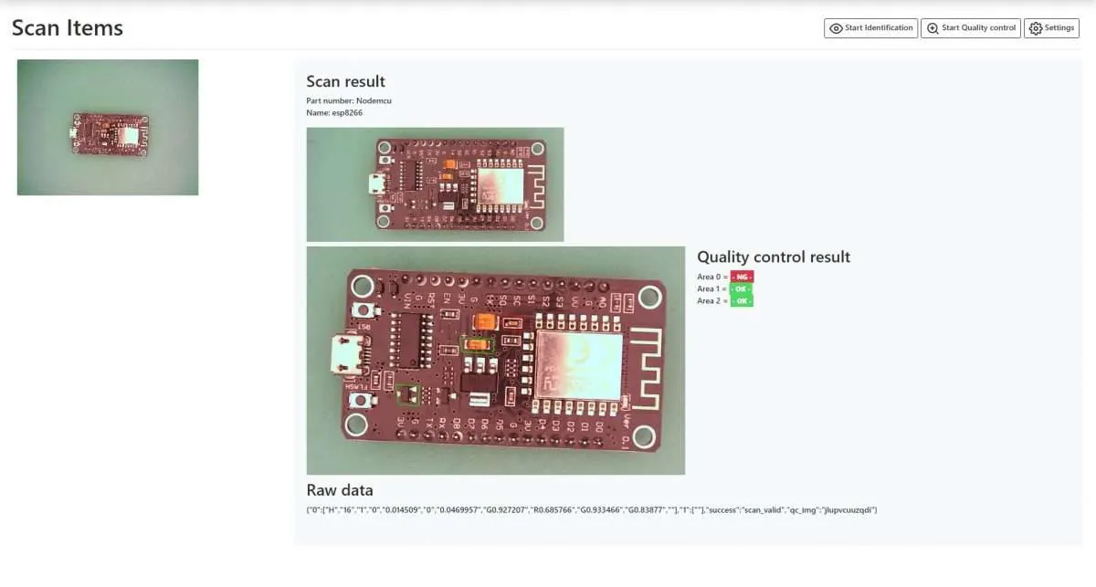
Why computer vision for PCBs and micro components?
Traditional manual inspection of PCBs and micro components is slow, inconsistent, and insufficient for modern electronics tolerances. A single missed solder bridge or misplaced component can cause field failures, recalls, and significant warranty costs. AI computer vision solves this with consistent, high-speed, objective inspection that scales with your production volume.
- 01
High precision
High-resolution cameras and advanced imaging detect defects invisible to the naked eye — down to micron-level anomalies.
- 02
100% consistency
Automated inspection eliminates variability introduced by human inspectors across shifts, fatigue levels, and experience gaps.
- 03
Real-time speed
Inspection cycles under 0.5 seconds per board — accelerating throughput without any compromise on accuracy.
- 04
Full traceability
Every inspection logged digitally — complete audit trail for quality management, compliance, and customer documentation.
Key applications in PCB & micro component inspection
AI vision can be deployed across multiple inspection points on the same production line for Building Supplies, with each inspection point targeting a specific failure mode to improve quality control and operational efficiency.
Solder joint inspection — detecting insufficient solder, bridges, cold joints, and voids.
Component placement verification — ensuring correct position, orientation, and polarity of every component.
Surface defect detection — scratches, cracks, contamination, corrosion, and delamination on micro components.
Trace & pad integrity — verifying circuit traces and pads meet design specs without breaks or shorts.
Dimensional measurement — measuring micro-scale features to confirm compliance with tight tolerances.
Missing component detection — flagging absent or wrong components before the board moves to the next stage.
Technologies and techniques used
High-resolution optical cameras with macro or microscopic lenses for sub-millimetre defect capture.
3D imaging & laser scanning for volumetric and surface profile analysis of solder joints and pad geometry.
Deep learning algorithms trained on your specific board designs — detecting complex defect patterns with no predefined limitations.
Infrared & X-ray imaging for non-visible defects — internal solder joint voids, hidden shorts, and subsurface cracks.

AI vision system autonomously inspecting a densely populated PCB — detecting solder defects, misalignment, and surface anomalies in real time.
Results of implementing AI vision in PCB QC
Manufacturers who deploy AI computer vision on their PCB lines consistently report four categories of measurable improvement:
Reduced scrap and rework costs by catching defects at the earliest possible stage
Improved product reliability and fewer field failures — better customer satisfaction and fewer warranty claims
Enhanced production efficiency — inspection time reduced by up to 90% vs manual checking
Scalable solution — same platform adapts to new product variants without hardware changes
- 01
Key metrics
Inspection speed <0.5s Tolerance ±0.1mm Defect reduction −35% Consistency 100% Deployment time 1 day Experts needed None
- 02
Industry
All AI QC solutions Electronics case studies Custom AI services
Related case studies
More real-world deployments across manufacturing industries.
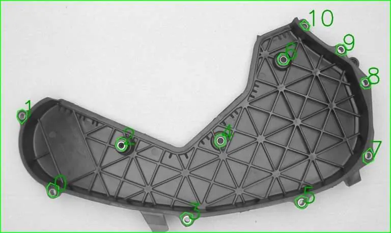
Case Study · Automotive Computer Vision & Injection Molding Read more

Case Study · Food How to reduce production waste with AI computer vision Read more
Case Study · Manufacturing
Computer Vision for Wood Inspection
Read more